In order to optimize the properties of each layer and, therefore, the characteristics of electronic devices, it is desirable to deposit each layer, and in particular the active semiconductor layer, in high purity conditions; therefore it is necessary to minimize all external sources of contamination as well as cross-contaminations among the different layers of the device.
Use of a UHV system which can achieve a good ultimate vacuum and, therefore, a low outgassing rate minimizes external sources of contamination, and there-by incorporation in the deposited films of residual impurities such as oxygen, nitrogen and carbon, which can have a detrimental effect on the properties of silicon thin films. Process Chambers (PC's) are constructed according to ultra high vacuum standards (stainless steel construction and all metal seals) which allow ultimate pressures in the 10-9 mbar range at room temperature and in the 10-7 mbar range at process temperature to be readily reached with turbomolecular pumping.
For a UHV system to maintain a good base vacuum with as little contaminants as possible it is desirable to keep the process chamber always under ultra-high vacuum conditions, using a load-lock chamber isolated from the process chamber by a gate valve; only the load-lock chamber is vented to atmosphere for substrate loading.
.gif)
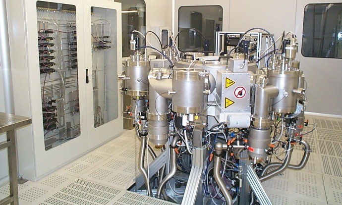
Cross contamination among different layers is avoided using a system configuration with multiple separate process chambers for the deposition of each layer with a specific gas mixture. The cluster multi-chamber configuration consists of multiple reaction chambers configured in a circular geometry; the contamination at the interface between layers is avoided using a central vacuum chamber connected to all process chambers to transfer the substrate from one process chamber to another without venting it, named transfer chamber (TC).
Multi-chamber cluster systems with a vacuum transfer chamber are commonly used for research and production of thin film devices. The vacuum transfer chamber is kept under vacuum during normal operation and a load lock chamber is used for substrate loading. Partially equipped or fully equipped 6-star configurations can accommodate up to 5 active chambers. Such designs allow for fewer active chambers while still able to accommodate more chambers for future requirements.
A typical 5-chamber cluster system could use RF PECVD in three process chambers (PC1 for intrinsic silicon, PC2 for doped silicon, PC4 for silicon alloys), Rapid Thermal Annealing by laser irradiation for crystallization in PC3 and plasma etching in PC5. The system features complete control by PC with capability of simultaneous independent operation of each process chamber as used for R&D on various types of thin film electronic devices
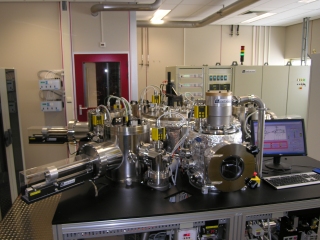
Research Level Clustertool
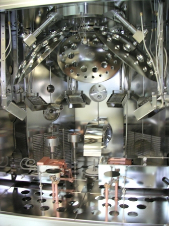
Box coater with planetary substrate holders / dual electron beam & thermal evaporation / dual magnetron sputter